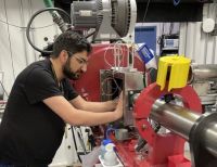
Using a five-year, $7.5 million grant from the U.S. Department of Defense, Johns Hopkins and Morgan State University are creating the Center for Advanced Electro-Photonics with 2D Materials, a first-of-its-kind initiative with a dual mission: to develop two-dimensional materials for use by DoD, and to expand and diversify the technology and defense-sector talent pipelines by training students from underrepresented minority groups. Operated in partnership with JHU's Applied Physics Laboratory, with support from scientists at the U.S. Army's Adelphi Laboratory Center and Aberdeen Proving Ground research centers, the new center is part of DoD's efforts to establish Centers of Excellence in Biotechnology and Materials Science at Historically Black Colleges and Universities.
Susanna Thon
Associate Professor, Whiting School of Engineering
"By furthering the relationship between our institutions ... we are creating pathways of success for students while increasing our research capacity in the area of next-generation materials for a variety of applications."
Key players from Johns Hopkins include Susanna Thon, associate professor in the Department of Electrical and Computer Engineering; Paulette Clancy, professor and head of the Department of Chemical and Biomolecular Engineering; Rama Venkatasubramanian, who leads the Energy and Thermal Management team in APL's Research and Exploratory Development Department; and David Shrekenhamer, a senior research scientist in APL's REDD.
"Johns Hopkins is pleased to be a partner with Morgan State on this initiative," Thon says. "By furthering the relationship between our institutions via the Center for Advanced Electro-Photonics with 2D Materials, we are creating pathways of success for students while increasing our research capacity in the area of next-generation materials for a variety of applications. We are especially excited about the potential to attract top-notch talent to and from within Baltimore, especially from groups underrepresented in science, technology, engineering, and mathematics, by combining the strengths of our two schools."
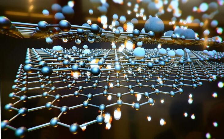
As part of the new center, researchers, and students will investigate properties of 2D materials for use in technologies to benefit warfighters. Two-dimensional materials are substances with a thickness of a few nanometers or less. (For reference, a sheet of paper is about 100,000 nanometers thick.) Students' experience working on these technologies will not only have an impact on their individual careers as engineers and scientists but will also benefit private and public sector industry, key organizers at Johns Hopkins say.
"Through the establishment of this center, STEM students have a space to perform cutting-edge research on an emergent class of quantum materials and technologies for clean energy, electromagnetic sensing, and information processing," Clancy says. "They also have the opportunity to create lasting relationships with researchers outside of their home institution. The impact this center will have on the workforce within the materials research community will be significant."
The cornerstone of the applied experience made available through the center's research will be summer internships for both Morgan and JHU students, co-advising of PhD dissertations, and joint annual workshops. Additional funding from the grant will underwrite internships for 10 to 15 undergraduate students and five students from area high schools and community colleges.
The joint research effort will target three specific areas of 2D materials technology: wearable photovoltaics and thermally managed photosensors augmented by plasmonic nanostructures; hybrid photovoltaics—thermoelectric technologies for the use of individual warfighters; and interrogation of quantum defects with light and quantized photogalvanic effects. These three research facets will be pursued in close coordination with scientists at APL and U.S. Army scientists at the Adelphi Laboratory Center and Aberdeen Proving Ground.
"The anticipated discoveries and breakthroughs in materials science and device physics will help lead to the next generation of quantum and image sensors," says Shrekenhamer. "APL has been a leader in attracting students from a diverse set of universities in the STEM area through an active intern program known as ATLAS—short for APL Technology Leadership Scholars—and this project collaboration with Morgan State and JHU will help further that objective."
Beyond their defense applications, 2D materials have universal functionality that can be used in many products and technologies, including high-efficiency solar cells, photosensors, and thermoelectric devices for waste-heat harvesting and refrigeration. The materials researched through the center will be synthesized at Morgan State. Members of the team at Johns Hopkins and APL will test and evaluate the 2D materials' stability and model both the rate at which they grow and their properties. The Johns Hopkins teams also will experiment with device development.
"The groundbreaking research in 2D electro-photonic materials and devices that will be performed in the new center will not only help to diversify the STEM talent pipeline for the U.S. DoD and members of industry, but it can also help develop innovative electronic and clean energy technologies of the future," Venkatasubramanian says. "Novel 2D materials engineered at the nanometer scale and efficient device architectures based on them are of great interest from a fundamental science point of view. An increase of knowledge in this field can potentially help break the bottlenecks faced by conventional materials of past decades."